- 您现在的位置:买卖IC网 > Sheet目录3822 > PIC18F4458-I/ML (Microchip Technology)IC PIC MCU FLASH 12KX16 44QFN
PIC18F2458/2553/4458/4553
DS39887C-page 20
2009 Microchip Technology Inc.
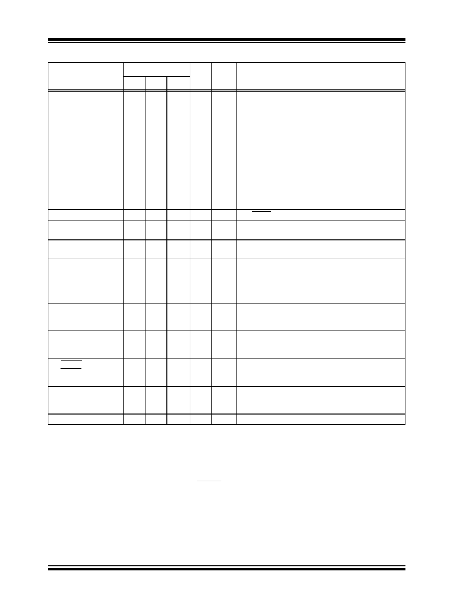
PORTE is a bidirectional I/O port.
RE0/AN5/CK1SPP
RE0
AN5
CK1SPP
825
25
I/O
I
O
ST
Analog
—
Digital I/O.
Analog input 5.
SPP clock 1 output.
RE1/AN6/CK2SPP
RE1
AN6
CK2SPP
926
26
I/O
I
O
ST
Analog
—
Digital I/O.
Analog input 6.
SPP clock 2 output.
RE2/AN7/OESPP
RE2
AN7
OESPP
10
27
I/O
I
O
ST
Analog
—
Digital I/O.
Analog input 7.
SPP output enable output.
RE3
—
See MCLR/VPP/RE3 pin.
VSS
12,
31
6, 30,
31
6, 29
P
—
Ground reference for logic and I/O pins.
VDD
11, 32 7, 8,
28, 29
7, 28
P
—
Positive supply for logic and I/O pins.
VUSB
18
37
O
P
—
Internal USB transceiver power supply.
When the internal USB regulator is enabled, VUSB is
the regulator output.
When the internal USB regulator is disabled, VUSB
is the power input for the USB transceiver.
NC/ICCK/ICPGC(3)
ICCK
ICPGC
——
12
I/O
ST
No Connect or dedicated ICD/ICSP port clock.
In-Circuit Debugger clock.
ICSP programming clock.
NC/ICDT/ICPGD(3)
ICDT
ICPGD
——
13
I/O
ST
No Connect or dedicated ICD/ICSP port clock.
In-Circuit Debugger data.
ICSP programming data.
NC/ICRST/ICVPP(3)
ICRST
ICVPP
——
33
I
P
—
No Connect or dedicated ICD/ICSP port Reset.
Master Clear (Reset) input.
Programming voltage input.
NC/ICPORTS(3)
ICPORTS
—
34
P
—
No Connect or 28-pin device emulation.
Enable 28-pin device emulation when connected
to VSS.
NC
—
13
—
No Connect.
TABLE 1-3:
PIC18F4458/4553 PINOUT I/O DESCRIPTIONS (CONTINUED)
Pin Name
Pin Number
Pin
Type
Buffer
Type
Description
PDIP QFN TQFP
Legend: TTL = TTL compatible input
CMOS = CMOS compatible input or output
ST = Schmitt Trigger input with CMOS levels
I
= Input
O
= Output
P
= Power
Note 1: Alternate assignment for CCP2 when CCP2MX Configuration bit is cleared.
2: Default assignment for CCP2 when CCP2MX Configuration bit is set.
3: These pins are No Connect unless the ICPRT Configuration bit is set. For NC/ICPORTS, the pin is No
Connect unless ICPRT is set and the DEBUG Configuration bit is cleared.
发布紧急采购,3分钟左右您将得到回复。
相关PDF资料
DSPIC33FJ64GP706A-I/PT
IC DSPIC MCU/DSP 64K 64-TQFP
PIC16F874-20/P
IC MCU FLASH 4KX14 EE 40DIP
DSPIC33FJ64GP706-I/PT
IC DSPIC MCU/DSP 64K 64TQFP
PIC24HJ128GP210-I/PT
IC PIC MCU FLASH 128KB 100TQFP
84854-101LF
METRAL 1000 RCPT 5ROW PRESS FIT
DIN-096SH-457
CONN DIN PLUG REAR 96POS
DSPIC30F4011-20I/P
IC DSPIC MCU/DSP 48K 40DIP
DSPIC30F4011-30I/P
IC DSPIC MCU/DSP 48K 40DIP
相关代理商/技术参数
PIC18F4458-I/P
功能描述:8位微控制器 -MCU 24KB Flash 2KB RAM RoHS:否 制造商:Silicon Labs 核心:8051 处理器系列:C8051F39x 数据总线宽度:8 bit 最大时钟频率:50 MHz 程序存储器大小:16 KB 数据 RAM 大小:1 KB 片上 ADC:Yes 工作电源电压:1.8 V to 3.6 V 工作温度范围:- 40 C to + 105 C 封装 / 箱体:QFN-20 安装风格:SMD/SMT
PIC18F4458-I/PT
功能描述:8位微控制器 -MCU 24KB Flash 2KB RAM RoHS:否 制造商:Silicon Labs 核心:8051 处理器系列:C8051F39x 数据总线宽度:8 bit 最大时钟频率:50 MHz 程序存储器大小:16 KB 数据 RAM 大小:1 KB 片上 ADC:Yes 工作电源电压:1.8 V to 3.6 V 工作温度范围:- 40 C to + 105 C 封装 / 箱体:QFN-20 安装风格:SMD/SMT
PIC18F4458T-I/ML
功能描述:8位微控制器 -MCU 24KB Flash 2KB RAM RoHS:否 制造商:Silicon Labs 核心:8051 处理器系列:C8051F39x 数据总线宽度:8 bit 最大时钟频率:50 MHz 程序存储器大小:16 KB 数据 RAM 大小:1 KB 片上 ADC:Yes 工作电源电压:1.8 V to 3.6 V 工作温度范围:- 40 C to + 105 C 封装 / 箱体:QFN-20 安装风格:SMD/SMT
PIC18F4458T-I/PT
功能描述:8位微控制器 -MCU 24KB Flash 2KB RAM RoHS:否 制造商:Silicon Labs 核心:8051 处理器系列:C8051F39x 数据总线宽度:8 bit 最大时钟频率:50 MHz 程序存储器大小:16 KB 数据 RAM 大小:1 KB 片上 ADC:Yes 工作电源电压:1.8 V to 3.6 V 工作温度范围:- 40 C to + 105 C 封装 / 箱体:QFN-20 安装风格:SMD/SMT
PIC18F4480-E/ML
功能描述:8位微控制器 -MCU 16 KB FL 768 RAM 36 I/O RoHS:否 制造商:Silicon Labs 核心:8051 处理器系列:C8051F39x 数据总线宽度:8 bit 最大时钟频率:50 MHz 程序存储器大小:16 KB 数据 RAM 大小:1 KB 片上 ADC:Yes 工作电源电压:1.8 V to 3.6 V 工作温度范围:- 40 C to + 105 C 封装 / 箱体:QFN-20 安装风格:SMD/SMT
PIC18F4480-E/P
功能描述:8位微控制器 -MCU 16 KB FL 768 RAM 36 I/O RoHS:否 制造商:Silicon Labs 核心:8051 处理器系列:C8051F39x 数据总线宽度:8 bit 最大时钟频率:50 MHz 程序存储器大小:16 KB 数据 RAM 大小:1 KB 片上 ADC:Yes 工作电源电压:1.8 V to 3.6 V 工作温度范围:- 40 C to + 105 C 封装 / 箱体:QFN-20 安装风格:SMD/SMT
PIC18F4480-E/PT
功能描述:8位微控制器 -MCU 16 KB FL 768 RAM 36 I/O RoHS:否 制造商:Silicon Labs 核心:8051 处理器系列:C8051F39x 数据总线宽度:8 bit 最大时钟频率:50 MHz 程序存储器大小:16 KB 数据 RAM 大小:1 KB 片上 ADC:Yes 工作电源电压:1.8 V to 3.6 V 工作温度范围:- 40 C to + 105 C 封装 / 箱体:QFN-20 安装风格:SMD/SMT
PIC18F4480-I/ML
功能描述:8位微控制器 -MCU 16KB FLASH 768 RAM 36 I/O 44P QFN RoHS:否 制造商:Silicon Labs 核心:8051 处理器系列:C8051F39x 数据总线宽度:8 bit 最大时钟频率:50 MHz 程序存储器大小:16 KB 数据 RAM 大小:1 KB 片上 ADC:Yes 工作电源电压:1.8 V to 3.6 V 工作温度范围:- 40 C to + 105 C 封装 / 箱体:QFN-20 安装风格:SMD/SMT